High-Density Interconnect PCBs (HDI PCBs) offer a superior wiring density compared to traditional through-hole designs, enabling advanced and compact electronic solutions. Defined under IPC-6012 standards, these PCBs feature an average of 20 or more electrical connections per square centimetre on each side, making them ideal for sophisticated, space-efficient applications.


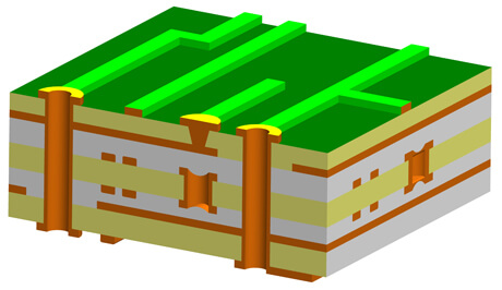
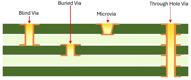
HDI technology supports the development of smaller, lighter, and highly reliable electronic devices by incorporating multiple layers, precise tracks, microvias, and blind or buried vias. With HDI, shorter signal paths minimise power loss and improve overall electrical performance. This enhanced performance makes HDI PCBs indispensable for high-speed signals and applications requiring robust signal integrity in cutting-edge technologies.
HDI PCB designs follow IPC-2226 guidelines, which specify key features that contribute to their advanced functionality:
| Feature | Technical Specification |
|---|---|
| Max Layer Count | 22, advanced 50 |
| PCB Thickness | 0.3mm - 4.5mm |
| PCB Size | 50 x 50mm - 700 x 600mm |
| Max Copper Thickness | Outer layer:6OZ Inner layer: 6OZ |
| Minimum Hole Size | 0.1mm, advanced 0.075MM |
| Max Hole Size | 3.5mm |
| Tighest Hole Tolerence | PTH:±0.075MM, NPTH:±0.05MM |
| Min Track Width | 0.762mm |
| Min Gap | 0.762mm |
| Finishes | OSP, ENIG, ENEPIG, EPAG, Immersion tin, Immersion Silver |
Sign up to receive a monthly PCB newsletter containing the latest information in the world of PCBS including new technology and supply chain information.
Sign up Now