Microwave & RF PCBs

High-Frequency Signals

PCBs designed for RF (Radio Frequency) and microwave applications are designed to handle extremely high-frequency signals, ranging from megahertz (MHz) to gigahertz (GHz). These circuits require precision engineering to minimise signal loss, interference, and distortion at these advanced frequencies.

Producing such PCBs involves specialised materials, as standard FR4 is unsuitable for frequencies above 1 GHz due to its higher losses and inconsistent dielectric properties. At Daleba, we excel in manufacturing high-performance RF and microwave PCBs either in the UK or by our Far East partners. Our extensive experience enables us to support clients across aerospace, defence, and telecommunications industries with accurate and dependable solutions. Every board of this type we create adheres to the strict demands of high-frequency environments, ensuring outstanding signal performance and long-lasting reliability, even in challenging conditions.

Industry Sectors
arrow
  • Medical
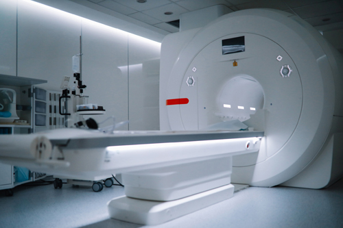
    Advanced imaging systems, such as MRI scanners, depend on RF/microwave PCBs for precise high-frequency signal generation and detection. For instance, proton imaging requires operation at 123 MHz.
  • Consumer Electronics
    Commonly used in Bluetooth devices, Wi-Fi routers, and smartphones, RF PCBs ensure reliable signal transmission in everyday wireless technologies.
  • Radar
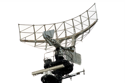
    RF PCBs are essential for radar technologies across multiple sectors:
    • In automotive applications, they support 77 GHz radar sensors for Advanced Driver Assistance Systems (ADAS).
    • In military systems, they enhance precision by detecting and tracking objects over long distances.
    • In aerospace, they enable long-range communications between satellites, ground stations, and aircraft for navigation and data transmission.
  • Telecoms
    RF PCBs play a crucial role in wireless communications, enabling high-frequency signal transmission and reception in devices like antennas, base stations, and RF amplifiers.
  • Satellite Communications
    High-frequency RF circuits are integral to satellite systems, supporting signal processing in ground stations and orbiting equipment. These PCBs ensure minimal signal loss in Ku-band frequencies (12-18 GHz).
Microwave RF RadarMicrowave RF Medical
Materials
arrow

Manufacturing RF and microwave PCBs requires specialised low-loss dielectric materials, including Rogers substrates, PTFE (Teflon), and ceramics. These materials are selected for their ability to maintain signal integrity at high frequencies.

Key material factors include:

  • Low and Stable Dielectric Constant (Dk): Ensures consistent signal performance by minimizing variations in signal propagation.
  • Low Loss Tangent: Reduces power loss to minimize signal attenuation. PTFE, known for its exceptional low loss tangent, is widely used in applications exceeding 5 GHz. It also offers superior chemical resistance and thermal stability.
  • Ceramic Substrates: Provide extremely low signal loss, excellent thermal stability, and a reliable coefficient of thermal expansion (CTE).

We have available materials from trusted manufacturers, including Rogers, Arlon, Nelco, Taconic, Ventec, and Isola, ensuring we can meet the specific requirements of each project.

Challenges of design and production
arrow
  • Stackup Design: Multi-layer PCBs, especially those using non-ceramic materials, are commonly employed to reduce interference and isolate high-frequency signals. Ground planes are frequently integrated to mitigate electromagnetic interference (EMI).
  • Thermal Management: High-frequency PCBs can generate substantial heat during operation. We offer expert guidance on effective thermal management solutions tailored to your design.
  • Impedance Control: Accurate impedance control is essential for ensuring consistent signal quality, achieved by minimising parasitic capacitance and optimising trace widths and spacing.
  • Manufacturing Precision: We specialise in the production of RF and microwave PCBs, delivering tight manufacturing tolerances. Our expertise ensures precise control over trace width and spacing, maintaining impedance and reducing signal loss.
  • Cost Considerations: Due to the use of specialised materials and precision processes, RF and microwave PCBs are typically more costly than standard PCBs.

RF Microwave Capabilities

Feature Specification
Layer Count 2 - 50
Key Technologies Controlled impedance, low loss materials, miniaturisation
Materials used Rogers, Arlon, Neclo, Taconic, Ventec and Isola, PPO, Teflon, Ceramic filled
Dielectric thickness 0.1mm – 3.0mm
Profile method Routing, v-score
Minimum track and gaps 0.075mm / 0.075mm (+/- 10% as per IPC)
Maxmimum dimensions 700mm x 600mm
Material thickness 0.4mm - 5.4mm
Surface finishes available HASL (Lead-free), OSP, ENIG, ENIPIG, Immersion tin, Immersion silver
Minimum laser drill 0.10mm standard, advanced NPTH ±0.05MM PTH:±0.075MM

Join Our Mailing List

Sign up to receive a monthly PCB newsletter containing the latest information in the world of PCBS including new technology and supply chain information.

Sign up Now
Joscar Registered