Daleba has developed a Direct Thermal Exchange Technology to aid modern thermal management issues of PCBs.
Electronics today are becoming more and more powerful with denser packaging and increased thermal management issues. The need to move heat away from components has never been greater. To achieve this the common method is to use conduction through the circuit to a heatsink or cold plate.
The efficiency of handling these thermal issues varies depending on the construction of the PCB and the Thermal Conductivity of the material used.
Ceramic substrate circuits are becoming more popular with their Thermal Conductivity values ranging from 24-180W/mK. The manufacturing constraints such as size and the cost of this new technology does not make it suitable for all applications. IMS (Insulated Metal Substrates) are a good solution for many. Initially introduced to combat rising junction temperatures of surface mount components on LEDs they consist of a thermally efficient electrically isolating dielectric layer between the copper tracks and an aluminium/copper base. Aluminium IMS tends to have a limit of between 8-10W/mK.
DTE – Direct Thermal Exchange Technology improves the thermal efficiency of IMS boards even further. The biggest thermal bottleneck of a metal core IMS is the dielectric, but with DTE the dielectric layer is bypassed by a plated, direct connection, through the dielectric to the base layer. These are sometimes called Pedestals. Thanks to this bypass, the heat can be transported with less thermal resistance, keeping the temperature of the component under control and extending its lifetime and operating performance. With their larger copper mass and efficiency, building pedestals will be more reliable compared to thermal vias ensuring a better spreading of the heat which allows for a better transfer to the heatsink.
The base layer for DTE has until now been copper which is heavy and expensive. Daleba offers DTE utilising a copper base but we have recently developed a technology where the plated copper connection can bond to an aluminium base providing the traditional heatsinking materials of copper to aluminium. Our technology ensures the DTE (pedestal) does not separate from the aluminium base and has passed 1,000 cycles for thermal shock.

Aluminium base DTE offers four distinct advantages over copper base DTE:


| Base Copper Weight (Thickness) | Standard | Special | |
|---|---|---|---|
| Minimum Track Width | 0.5oz (18um) | 0.10 | <0.10 |
| 1oz (35um) | 0.10 | <0.10 | |
| 2oz (70um) | 0.20 | <0.20 | |
| 3oz (105um) | 0.25 | <0.25 | |
| Minimum Track Gap | 0.5oz (18um) | 0.10 | <0.10 |
| 1oz (35um) | 0.15 | <0.15 | |
| 2oz (70um) | 0.20 | <0.20 | |
| 3oz (105um) | 0.25 | <0.25 |
| Hole Data | Standard | Special |
|---|---|---|
| Minimum Hole Size | 1.20 | N/A |
| Hole Tolerance - Drilled | ±0.05 | ±0.03 |
| Hole Tolerance - Routed Holes | ±0.10 | +0 /-0.05 |
| Minimum Hole to Edge | 0.10 | <0.10 |
| Hole to Edge Tolerance | ±0.15 | ±0.10 |
| Minimum Radial Clearance Pad (Annulus) | 0.1 | 0.75 |
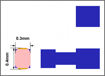 Min Pedestal Size
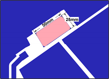 Max Pedestal Size
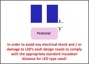 Pedestal Gap
Copper to Aluminium bond has passed the 1000 cycle test for thermal shock.
| Number of Test Cycle (NCYCLE) | 1000 |
| Minimum Chamber Temperature (Tmin) | -40°C |
| Maximum Chamber Temperature (Tmax) | +125°C |
| Transfer Time (t2) between Chambers | ≤10 S |
| Dwell Time (t) at low/high temp | 15 minutes |

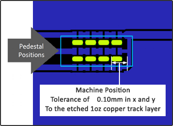
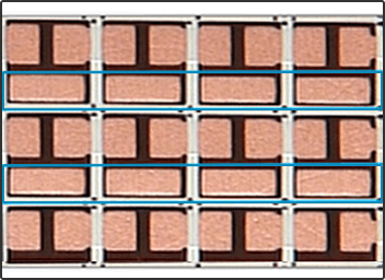
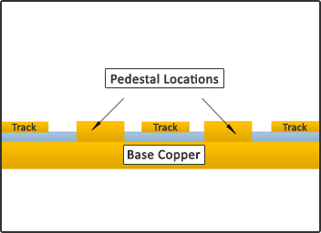

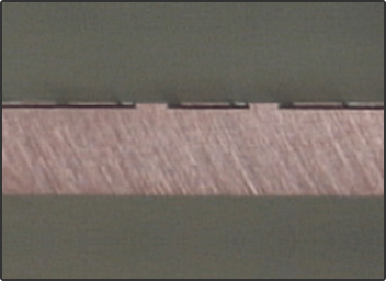
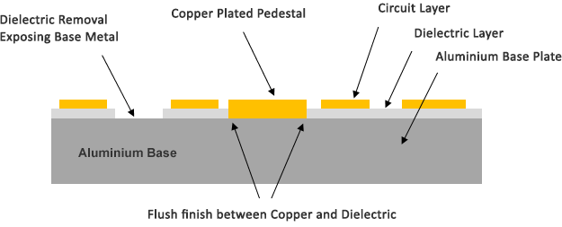
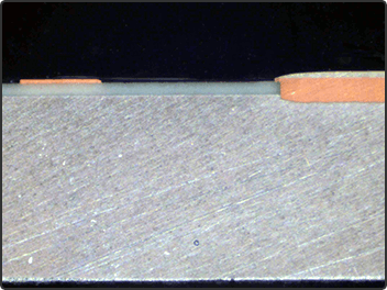
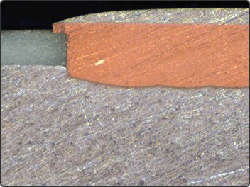
These images show Daleba's unique DTE technology with a copper pedestal plated through the dielectric to produce a permanent bond to the aluminium base.
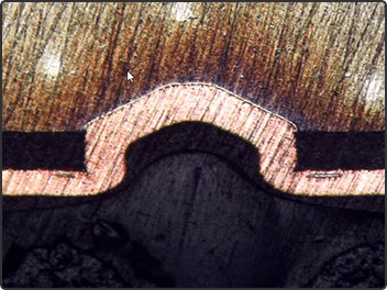
Can also be used for current, a micro via for electrical contact - copper layer to aluminium which allows the base layer to be a ground layer. The above microsection was produced after 1000 cycle test for thermal shock.
Sign up to receive a monthly PCB newsletter containing the latest information in the world of PCBS including new technology and supply chain information.
Sign up Now