Daleba recently worked on a unique project for Fraunhofer Institute for Solar Energy Systems ISE.
https://www.ise.fraunhofer.de/en/business-areas/power-electronics-and-grids.html
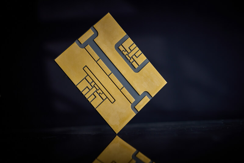
Ceramic PCB
We are delighted to have found Daleba, whose unique manufacturing capabilities for Ceramics allowed them to produce our specialised PCB precisely to our requirements. From the outset, their team provided clear and straightforward communication, ensuring that every detail of our specifications was understood. Their responsiveness and commitment to meeting our needs were exceptional. The boards were delivered on time, exactly as specified, and to the highest quality standards. We look forward to working with Daleba again in the future.
The actual DPC ceramic board is used for a novel power module design for gallium nitride (GaN) transistors. Please find more details on this in our research article: https://doi.org/10.1002/ente.202300460.
The four GaN bare dies are double-sided sintered between two ceramic substrates for low CTE mismatch and high durability at elevated temperatures. The ceramic material for the upper substrate is chosen to be silicon nitride (Si3N4). It has the same CTE of 2.6 ppm/K as Si which is the substrate material for the GaN bare die, close to the CTE of GaN with 3.2 ppm/K.
Si3N4 has a high rupture strength which allows for a low material thickness of 250µm at a copper thickness of 300µm. This minimizes the stray inductance of the power loop.
Vias through the upper ceramic substrate are necessary to achieve low-inductive power and gate loops. For a high current-carrying capacity of 300 A, copper-filled vias are preferred to reduce the necessary number of vias in the power loop. Different copper thicknesses on the bottom-side of the upper substrate are advantageous for the application of the epoxy around the edges of the bare dies since the gap size is increased.
Thanks again to the Team at Daleba and we forward to working with you again in the future.
Date : 19-03-2025
Sign up to receive a monthly PCB newsletter containing the latest information in the world of PCBS including new technology and supply chain information.
Sign up Now
Daleba can manufacture PCBs ranging from single-sided to complex boards in excess of 40x layers. Our in-house CAM engineering resource allows us to rapidly check, panelise and commercially optimise a fast turnaround prototype as well as small volumes. We can supply simple technology boards in as little as 24 hours!


