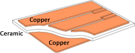
Active Metal Brazing (AMB) is the latest developments in ceramic substrates and offers the ability to produce Heavy Copper with a AlN (Aluminium Nitride) or SiN (Silicon Nitride). The normal metallisation process is not used as AMB involves brazing pure copper on the ceramic in a high temperature vacuum brazing process. As well as offering a high reliability substrate with unique heat dissipation. The brazing technology also enables double sided copper weights of up to 800µm on thin ceramic substrates of just 0.25mm

Thick copper on a ceramic substrate with a thermal conductivity of up to 180 W/mK, high heat capacity and a low CTE make AMB ideal for Power Electronic applications.
Ceramics - AMB (Active Metal Brazing)
AMB Single Sided
Various copper weights are available to meet match substrate thicknesses detailed in the table below. It is recommended the copper thickness on any design is no more than half the ceramic thickness.
AMB double sided
Double sided substrates offer greater mechanical strength and stability enabling Heavy Copper to be offered on thin ceramic substrates. The following is a guide on double sided material availability although during the etching process original copper weights can be reduced.
| Active Metal Brazing Double Sided Panels | ||||||
|---|---|---|---|---|---|---|
| 200µm | 250µm | 300µm | 400µm | 500µm | 800µm | |
| 0.25mm | SiN AlN |
SiN AlN |
SiN | SiN | SiN | SiN |
| 0.32mm | SiN | SiN | SiN | SiN | SiN | SiN |
| 0.38mm | AlN | AlN | AlN | |||
| 0.63mm | AlN | AlN | AlN | AlN | AlN | |
| 1.00mm | AlN | AlN | AlN | AlN | AlN | AlN |
Ceramic - Capabilities
| Property | AMD | DPC | DBC |
|---|---|---|---|
| Compatible Substrates | AlN / SiN | Al2O3 / AlN / SiN | Al2O3 / AlN / SiN |
| Substrate Thickness (mm) | 0.25/0.32/0.38/0.63/1.0mm.1.0 | 0.25/0.38/0.5/0.635.1.0/1.5/2.0 | 0.25/0.38/0.5/0.635.1.0/1.5/2.0 |
| Copper Weight (oz) | See Below | 10 - 140 | 140 - 350 |
| Panel Sizes (mm x mm) | Standard: 115 x 115mm Special: Up to 170 x 250mm |
Standard: 115 x 115mm Special: Up to 170 x 250mm |
Standard: 115 x 115mm Special: Up to 170 x 250mm |
| Finish Options | ENIG/ENEPIG/EPIG/Immersion Silver/Immersion Tin/OSP | ENIG/ENEPIG/EPIG/Immersion Silver/Immersion Tin/OSP | ENIG/ENEPIG/EPIG/Immersion Silver/Immersion Tin/OSP |
| Min Track Width (mm) | Dependant on Cu Weight | 0.1 | Dependant on Cu Weight |
| Minimum Hole Dia (mm) | 0.08 | 0.08 | 0.08 |
| Plated Via Aspect Ratio | N/A | 5:1 | N/A |
Note: Through hole plating is not possible with AMB or DBC substrates.
Click here for more information on AMB
Date : 08-07-2021
Sign up to receive a monthly PCB newsletter containing the latest information in the world of PCBS including new technology and supply chain information.
Sign up Now